- The researchers demonstrated a transparent, flexible silicon-photonics platform at the 300-millimetre wafer scale.
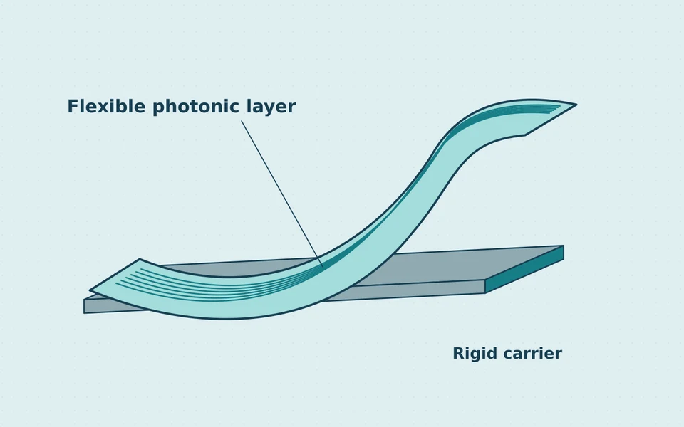
- They patterned the optical components on a rigid base before transferring the working layers to a transparent film.
- Repeated bending preserved performance down to a tested radius, with degradation at a tighter bend.
Inside this story 2 perspectives
Making an optical circuit that can wrap around a curve starts, rather unexpectedly, with a surface that must stay flat. This week researchers at MIT described how they and engineers at the Albany NanoTech Complex made a wafer that is both transparent and flexible while using the methods of a semiconductor foundry. The trick was deciding when the familiar rigid silicon base had finished its job.
Silicon photonics uses small structures called waveguides to carry light across a chip. Their paths have to be patterned precisely. A stiff, even base helps a factory place those paths where they belong, but is a poor fit for a device intended to follow the curve of a display or sit discreetly against skin. Previous work had shown that individual chips could be made flexible or transparent. This team tackled both properties on a wafer 300 millimetres across.
A support that leaves the finished device
The researchers first deposited and patterned the optical structures on a conventional silicon substrate. They bonded a temporary wafer on top, flipped the assembly over and removed the original base. A thin, transparent polyester film could then support the layers that contained the waveguides. Releasing the temporary support left those functional layers on a surface that could bend.
Doing this once to a small specimen and doing it across a large disc impose different demands. Stress can make a wafer bow. Remove slightly too much material in one place and a delicate optical structure can be damaged. Leave too much over a wide area and the chip keeps some of the stiffness or opacity the process is supposed to remove. The team combined industrial thinning with a more selective final removal step to protect the working layers.
What the bend tests could show
A transparent device has to work in two directions at once. The intended light signal has to travel along its optical path. At the same time a person looking through the surface should still be able to see what lies beyond it. The researchers assessed the quality of the view through the chip as well as whether the optical structures kept performing when bent.
They repeatedly wrapped a chip around cylinders of several diameters. It retained performance through thousands of bends in the reported tests, including at a diameter comparable to a small screw. Repeated bending around a still narrower object, about the size of a toothpick, began to cause degradation. Both observations matter to a designer choosing how sharply a device can curve.
A comfortable wearable or a transparent display would still need its other components, packaging and real-use testing. The advance here is in how the optical part can be manufactured. A foundry can begin with a format it knows how to handle and finish with a sheet whose mechanical properties are quite different.